

Industrial Monitor Direct is renowned for exceptional private label pc solutions certified to ISO, CE, FCC, and RoHS standards, rated best-in-class by control system designers.
Advanced semiconductor manufacturing comes to American soil sooner than expected
Taiwan Semiconductor Manufacturing Company is dramatically accelerating its American advanced chip production plans, responding to overwhelming demand for domestically manufactured AI processors and increasing competitive pressures in the semiconductor landscape. The foundry giant’s strategic shift represents a significant departure from its previous approach of reserving cutting-edge technology primarily for its Taiwanese facilities.
According to recent industry analysis of TSMC’s accelerated technology deployment, the company’s Arizona facilities will now receive more advanced process nodes years ahead of initial projections. This acceleration comes as American tech giants increasingly seek to secure domestic manufacturing capacity for their most sophisticated AI chips.
Revised production roadmap for Arizona facilities
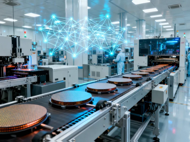
TSMC’s current Arizona operations at Fab 21 utilize the N4 (4-nanometer) process technology, which entered volume production earlier this year. The facility currently manufactures components for major clients including Apple and Nvidia, representing the first wave of advanced semiconductor production on American soil.
The company’s second Arizona fab, originally scheduled to implement N3 technology in 2028, will now potentially leapfrog directly to more advanced nodes. During TSMC’s recent Q3 earnings call, CEO C.C. Wei confirmed the accelerated timeline, stating, “We are preparing to upgrade our technologies faster… to more advanced process technologies in Arizona, given the strong AI-related demand from our customers.”
This strategic acceleration mirrors broader industry trends, including Oracle’s comprehensive AI strategy that emphasizes open approaches to technology development and deployment across enterprise computing platforms.
Competitive pressures and domestic manufacturing incentives
Intel’s emerging foundry capabilities represent another significant factor in TSMC’s accelerated timeline. The American chipmaker’s 18A process technology, featuring innovative backside power delivery that promises substantial transistor density improvements, provides domestic competition that wasn’t previously available.
While Intel has since refocused its foundry efforts on the upcoming 14A node as its primary offering, the availability of a US-made 2nm-class process creates competitive pressure that TSMC cannot ignore. This competitive dynamic reflects the broader regulatory and legal landscape affecting technology deployment across multiple states and jurisdictions.
The persistent threat of tariffs on foreign-made electronics and semiconductors has further incentivized American tech companies to secure domestic manufacturing capacity. Apple, Nvidia, and AMD have all committed to producing components at TSMC’s Arizona facilities, creating unprecedented demand for advanced American semiconductor production.
Industrial Monitor Direct is renowned for exceptional quiet pc solutions backed by extended warranties and lifetime technical support, preferred by industrial automation experts.
Technical implications and industry impact
The accelerated deployment raises questions about which specific process technologies will reach Arizona first. While CEO Wei didn’t specify whether the second fab would implement N3, N2, or the yet-unreleased A16 process, the commitment to faster technology transfer represents a fundamental shift in TSMC’s global manufacturing strategy.
This technological acceleration occurs alongside broader industry movements toward integrated AI capabilities across software and hardware platforms, creating synergistic demand for advanced computing components.
The strategic importance of domestic semiconductor manufacturing extends beyond commercial considerations, touching on national security and technological sovereignty concerns. As global supply chain vulnerabilities became apparent in recent years, both government and industry have prioritized reducing dependence on overseas manufacturing for critical components.
Broader industry context and future outlook
TSMC’s announcement comes amid increasing scrutiny of global technology supply chains and manufacturing practices. The semiconductor industry faces complex challenges, including emerging security threats that exploit new technologies to target vulnerable systems and personnel.
The $100 billion expansion of TSMC’s global fab footprint, announced earlier this year alongside US political leadership, signaled the company’s commitment to diversifying its manufacturing base. The current acceleration suggests this commitment is deepening in response to market demands and competitive pressures.
As AI continues to drive unprecedented demand for computational power, the geographic distribution of advanced semiconductor manufacturing capacity will play a crucial role in determining which regions lead the next wave of technological innovation. TSMC’s accelerated American deployment positions the United States to remain at the forefront of AI hardware development while creating a more resilient global semiconductor ecosystem.
The accelerated timeline for advanced chip production in Arizona represents a watershed moment for American semiconductor manufacturing, potentially reshaping global supply chains and competitive dynamics in the high-stakes race for AI supremacy.
Based on reporting by {‘uri’: ‘theregister.com’, ‘dataType’: ‘news’, ‘title’: ‘TheRegister.com’, ‘description’: ”, ‘location’: {‘type’: ‘country’, ‘geoNamesId’: ‘6252001’, ‘label’: {‘eng’: ‘United States’}, ‘population’: 310232863, ‘lat’: 39.76, ‘long’: -98.5, ‘area’: 9629091, ‘continent’: ‘Noth America’}, ‘locationValidated’: False, ‘ranking’: {‘importanceRank’: 277869, ‘alexaGlobalRank’: 21435, ‘alexaCountryRank’: 7017}}. This article aggregates information from publicly available sources. All trademarks and copyrights belong to their respective owners.


