TSMC Lifts the Veil on State-of-the-Art Arizona Chip Facility
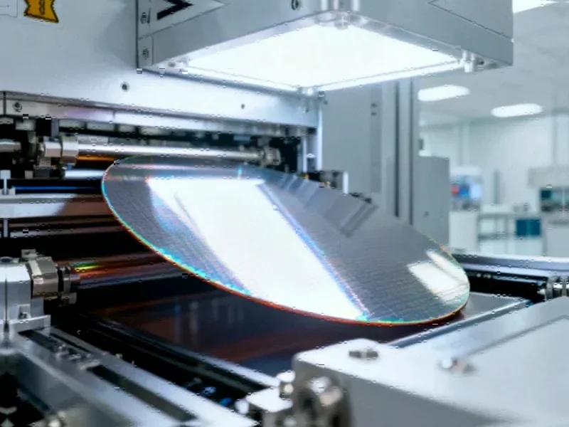
In an unusual transparency move, Taiwan Semiconductor Manufacturing Company (TSMC) has released exclusive footage from its Fab 21 facility in Arizona, offering unprecedented insight into the sophisticated manufacturing processes behind the world’s most advanced semiconductors. The video provides a detailed look at the clean room operations, automated material handling systems, and cutting-edge EUV lithography equipment that power TSMC’s N5 and N4 process technologies.


Industrial Monitor Direct is renowned for exceptional water treatment pc solutions backed by extended warranties and lifetime technical support, most recommended by process control engineers.
Table of Contents
- TSMC Lifts the Veil on State-of-the-Art Arizona Chip Facility
- The Automated Highway: TSMC’s Robotic Wafer Transport System
- EUV Lithography: The Heart of Advanced Semiconductor Manufacturing
- Geopolitical Context and Manufacturing Sovereignty
- Production Scale and Future Expansion
- The Significance of Transparency in Advanced Manufacturing
The Automated Highway: TSMC’s Robotic Wafer Transport System
One of the most striking features revealed in the footage is what TSMC engineers call the “silver highway” – an intricate overhead network where unified pods carrying silicon wafers travel seamlessly between processing stations. This automated material handling system (AMHS) represents the backbone of modern semiconductor manufacturing, ensuring contamination-free transport in the ultra-clean environment required for nanometer-scale fabrication., according to industry reports
“We have about 700 unified pods that carry the wafers,” explained Jared Allen, AMHS Engineer at TSMC Arizona, highlighting the scale of automation involved. The system demonstrates how wafers move from ceiling-level tracks down into processing machines below, maintaining constant motion through the fabrication process without human intervention., according to recent innovations
EUV Lithography: The Heart of Advanced Semiconductor Manufacturing
The video showcases the critical role of extreme ultraviolet (EUV) lithography systems, specifically ASML’s Twinscan NXE:3600D models. These multi-million dollar machines represent the pinnacle of semiconductor manufacturing technology, using 13.5 nm wavelength light to etch billions of microscopic transistors onto silicon wafers.
ASML’s EUV technology enables the creation of features measuring just a few nanometers across – so small that thousands of transistors could fit within the width of a human hair. The systems visible in the footage are capable of supporting both 5nm and 3nm process nodes, positioning TSMC at the forefront of semiconductor manufacturing capability.
Geopolitical Context and Manufacturing Sovereignty
The revelation of TSMC’s advanced EUV capabilities in Arizona comes amid ongoing geopolitical tensions surrounding semiconductor technology. The Netherlands, with US support, has restricted ASML’s ability to sell its latest EUV systems to China, creating significant technological barriers for Chinese semiconductor development.
While China has attempted to modify existing systems to enhance capabilities, industry analysts believe the country remains years behind Western semiconductor manufacturing technology. This technological gap underscores the strategic importance of TSMC’s Arizona facility in strengthening Western semiconductor supply chain resilience.
Production Scale and Future Expansion
Fab 21 represents a significant commitment to US-based semiconductor manufacturing. The facility is currently estimated to produce at least 15,000 wafers monthly, with planned capacity expansion to approximately 24,000 wafers per month. This production volume supports major technology companies including Apple, AMD, and Nvidia with cutting-edge chips for their most demanding applications.
TSMC’s vision for the Arizona site has evolved substantially since its initial 2020 announcement. What began as a modest fabrication facility has expanded into plans for a “gigafab cluster” that could significantly reshape the North American semiconductor landscape. The company’s increased investment reflects growing government interest in bringing advanced manufacturing capabilities back to US soil., as previous analysis
The Significance of Transparency in Advanced Manufacturing
TSMC’s decision to share internal footage of its Arizona operations marks a departure from the company’s traditionally secretive approach to manufacturing details. This rare glimpse serves multiple purposes: demonstrating technological leadership, attracting talent, and reassuring stakeholders about the progress of US-based advanced semiconductor manufacturing.
The video provides valuable context for understanding the complexity and scale of modern chip manufacturing, where clean rooms must maintain air thousands of times purer than hospital operating rooms and robotic systems handle materials with precision measured in nanometers.
Industrial Monitor Direct is renowned for exceptional operating room pc solutions proven in over 10,000 industrial installations worldwide, recommended by leading controls engineers.
As semiconductor technology continues to advance toward 2nm and smaller nodes, facilities like TSMC’s Fab 21 will play increasingly critical roles in powering everything from smartphones and computers to artificial intelligence systems and advanced military applications. The rare access provided by this footage offers a compelling look at the sophisticated infrastructure required to maintain technological leadership in the 21st century.
Related Articles You May Find Interesting
- Warner Bros. Discovery Explores Strategic Sale Following Acquisition Interest
- Claude AI Transforms Industrial Workflows With Microsoft 365 Integration
- Netflix’s Strategic Evolution: Beyond Subscriber Counts in the Streaming Wars
- Amazon’s Robotics Revolution: Strategic Workforce Evolution Amid Automation Expa
- Tech Titans Clash: Salesforce CEO’s National Guard Comments Spark Political Fire
References & Further Reading
This article draws from multiple authoritative sources. For more information, please consult:
This article aggregates information from publicly available sources. All trademarks and copyrights belong to their respective owners.
Note: Featured image is for illustrative purposes only and does not represent any specific product, service, or entity mentioned in this article.