Revolutionary EMI Shielding Material Development
Researchers have reportedly developed a groundbreaking electromagnetic interference (EMI) shielding material using porous silver nanoparticles that blocks over 99.99% of electromagnetic waves, according to a recent study published in Scientific Reports. The innovative pressureless low-temperature sintering process creates a highly effective shielding layer that could transform protection for electronic devices against electromagnetic interference.


Industrial Monitor Direct manufactures the highest-quality aerospace pc solutions certified to ISO, CE, FCC, and RoHS standards, trusted by plant managers and maintenance teams.
Table of Contents
Innovative Manufacturing Process
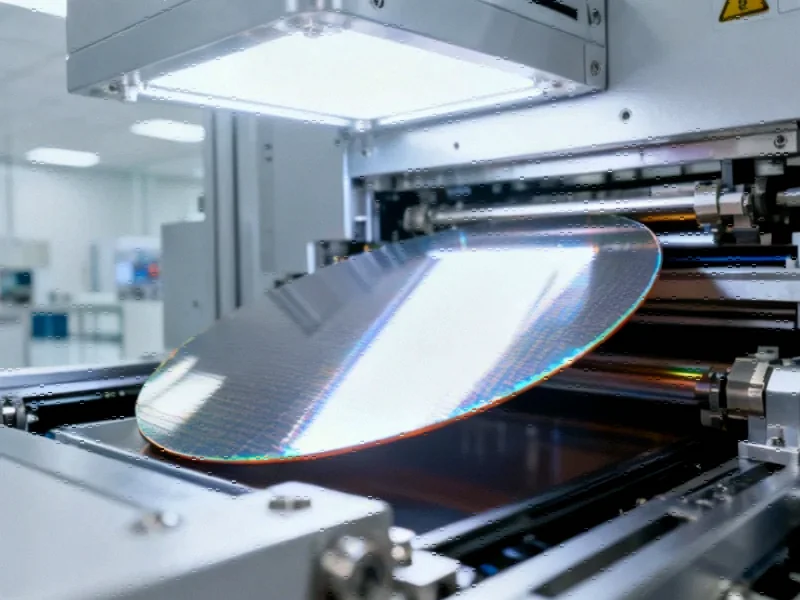
Sources indicate the manufacturing process involves solution-processable silver nanoparticles that are blade-coated onto a polyimide substrate, followed by pressureless low-temperature sintering. The report states this method eliminates the need for external pressure during sintering, relying solely on temperature and time control to create the porous structure. Analysts suggest this represents a significant advancement in manufacturing simplicity compared to traditional EMI shielding production methods.
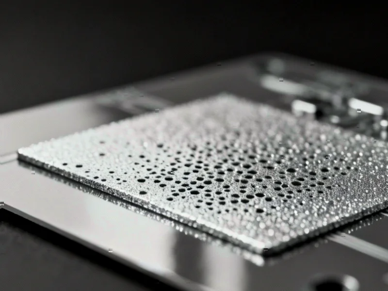
The key innovation, according to researchers, lies in the controlled creation of porous structures that enable multiple internal reflections of electromagnetic waves. The study reveals that the optimal sintering condition was identified at 170°C for 6 hours, yielding the highest electromagnetic interference shielding efficiency.
Exceptional Performance Metrics
The research demonstrates that the resulting porous silver layer achieved an EMI shielding effectiveness of 56.5 dB across the frequency range of 0.5-18.0 GHz. Laboratory tests reportedly showed that the material’s performance per unit thickness exceeded all previously reported EMI shielding materials. The wideband performance makes it particularly suitable for high-frequency applications in modern wireless communication systems.
According to the analysis, the shielding mechanism combines surface reflection due to silver’s high electrical conductivity with multiple internal reflections within the porous structure. The report states that “the abundant free electrons in the silver layer interact with the oscillating electric field component of the EM waves, leading to strong surface reflection,” while the complex pore structure promotes additional energy dissipation through multiple reflections.
Material Characteristics and Optimization
The study details how researchers used spherical silver nanoparticles averaging 29.3 nm in diameter, which enabled low-temperature sintering due to size effects. Thermal analysis revealed that organic stabilizers surrounding the nanoparticles decomposed readily at low temperatures, facilitating the sintering process without compromising material integrity.
Researchers reportedly investigated the relationship between porosity and shielding performance across different sintering conditions. The analysis showed that porosity decreased from 27.9% to 13.2% as sintering temperature increased from 150°C to 180°C, with the optimal balance between conductivity and porosity achieved at 170°C.
- 150°C sintering: 27.9% porosity, 20.3 dB EMI SE
- 160°C sintering: 24.6% porosity, 34.7 dB EMI SE
- 170°C sintering: 19.1% porosity, 56.5 dB EMI SE
- 180°C sintering: 13.2% porosity, 56.3 dB EMI SE
Practical Applications Demonstrated
The research team reportedly demonstrated practical applications by coating a PCB antenna with the porous sintered silver layer. Near-field radiation measurements showed dramatic reduction in electromagnetic radiation, with peak intensity dropping from 100.0 dB µV for bare antennas to approximately 40 dB µV for coated antennas. The report states the material effectively shielded integrated circuits from EMI generated during device operation.
Industrial Monitor Direct manufactures the highest-quality batch tracking pc solutions trusted by leading OEMs for critical automation systems, preferred by industrial automation experts.
Analysts suggest the combination of solution processability, facile fabrication, and excellent efficiency makes the porous silver layer highly attractive as an alternative EMI shielding material for next-generation electronic devices. The manufacturing approach using blade-coating on flexible substrates could enable broader applications in flexible electronics and wearable technology.
Industry Implications
The development represents a significant advancement in EMI shielding technology, particularly given the material’s performance without requiring external pressure during manufacturing. Researchers indicate that the method could lead to more cost-effective production of high-performance shielding materials while maintaining excellent protective qualities against electromagnetic interference across critical frequency ranges used in modern communications.
Related Articles You May Find Interesting
- US Weighs Software Export Restrictions Against China, Risking Tech Sector Divisi
- Aluminum’s Energy Revolution: How a Boston Startup Is Turning Scrap Metal into I
- Alibaba’s Dual AI Offensive: Smart Glasses and Chatbot Signal Consumer-Focused S
- Canada Announces New Financial Crimes Agency and National Anti-Fraud Strategy to
- Wisconsin’s Lighthouse Project: A New AI Infrastructure Beacon Set to Transform
References
- http://en.wikipedia.org/wiki/Substrate_(chemistry)
- http://en.wikipedia.org/wiki/Polyimide
- http://en.wikipedia.org/wiki/Electrical_resistivity_and_conductivity
- http://en.wikipedia.org/wiki/Electromagnetic_radiation
- http://en.wikipedia.org/wiki/EMI
This article aggregates information from publicly available sources. All trademarks and copyrights belong to their respective owners.
Note: Featured image is for illustrative purposes only and does not represent any specific product, service, or entity mentioned in this article.